 Scanning Electron Microscopy (SEM)
Overview
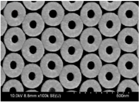
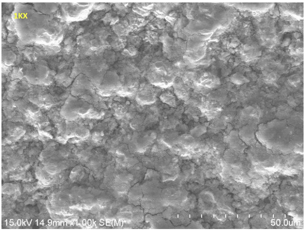
Scanning Electron Microscopy Analysis (SEM) is a high-resolution imaging and elemental analysis technique that delivers insights into the topography, morphology, and composition of materials. It functions by directing a focused beam of high-energy electrons onto a sample’s surface, generating secondary electrons, backscattered electrons, and characteristic X-rays. These signals are captured by detectors, enabling detailed imaging and elemental identification.
SEM’s exceptional nanoscale resolution allows us to visualize features as small as a few nanometers, making it indispensable in materials science, biology, and various other fields. Whether you’re exploring microelectronics, studying biological specimens, or analyzing advanced materials, SEM offers versatile applications.
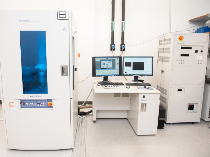
At Outermost Technology, our SEM Analysis services provide precise imaging and elemental analysis capabilities. With state-of-the-art equipment and experienced analysts, we deliver high-quality data for your research, failure analysis, or materials optimization needs.
Explore the advantages of SEM Analysis, discover its diverse applications, and see how our services can enhance your material characterization requirements. Join us on an exciting journey to explore the micro and nanoscale worlds through Scanning Electron Microscopy.
Services
- (cross-sectional) SEM
- (cross-sectional) SEM-EDS
- (cross-sectional) SEM-EBSD
Pricing
- Regular service: Starts from $250 per sample with 4 – 5 days turnaround.
- Relaxed service: Starts from $200 with 7 – 10 days turnaround.
- For a comprehensive overview of our pricing structure, please log in to the Bee Portal.
Equipment
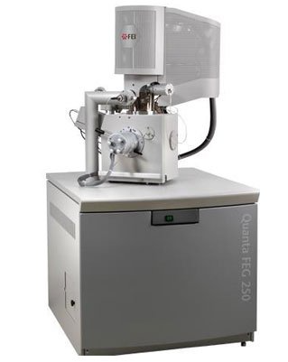
- 0.4 nm resolution at 30 kV (Highest SEM resolution guarantee in the world)
- 1.6 nm resolution at 1 kV
- Magnification range of 60X – 2,000,000X
- Patented SE/BSE detector mode for signal mixing
- Unique BF/DF Duo-STEM detector option
- Diverse specimen holders, compatible with FIB and STEM

- High resolution Schottky field emission
- SEM column optimized for high brightness/high current.
- High vacuum imaging with beam deceleration up to 4 kV: Landing energy: 200 V to 30 kV
- Imaging resolution in high vacuum mode at 30 kV: 0.8 nm (STEM), 1.0 nm (SE), 2.5 nm (BSE)
- Wet STEM stage for viewing TEM samples/ ESEM samples
- 3 nm SE resolution at 1 kV in high vacuum mode and at 3 kV in low-vacuum mode
- Imaging resolution in low vacuum mode at 30 kV: 1.4 nm (SE), 2.5 nm (BSE)
- Oxford Silicon drift detector (SDD) with 150 mm window for EDS
- Oxford EBSD system for grain orientation mapping
- Oxford Aztec software for EDS and EBSD
- Maximum horizontal field width: 5 mm at analytical working distance of 10 mm; 18.8 mm at 65 mm WD
- Probe current: ≤ 200 nA, continuously adjustable
- Magnification: 6 to 1000000x

FAQ
A: Scanning Electron Microscopy (SEM) analysis is an advanced imaging and analytical technique that uses a focused beam of high-energy electrons to visualize and characterize the surface morphology and composition of materials at a nanoscale level.
A: SEM works by directing a focused electron beam onto the surface of a sample. When the electrons interact with the atoms at the surface, they generate various signals, including secondary electrons, backscattered electrons, and characteristic X-rays. Detectors capture these signals to create detailed images and provide elemental information.
A: SEM can analyze a wide range of samples, including metals, ceramics, polymers, biological specimens, geological materials, and advanced composites. It is particularly useful for examining surface features and structures.
A: SEM offers several advantages, including higher resolution, greater depth of field, and the ability to examine non-conductive and irregularly shaped samples. It provides detailed surface information and can visualize structures at the nanoscale level.
A: SEM analysis provides information about the topography, morphology, and elemental composition of a sample’s surface. It can reveal features such as surface roughness, particle size and distribution, and the presence of contaminants or elements.
A: In materials science and research, SEM is employed to investigate the microstructure of materials, study defects, analyze fractured surfaces, examine coatings, and assess the quality of materials. It aids in understanding material properties and behavior.
A: SEM finds applications in various industries, including electronics, aerospace, automotive, and pharmaceuticals. It is used for quality control, failure analysis, product development, and process optimization.
A: Yes, SEM can provide elemental analysis through energy-dispersive X-ray spectroscopy (EDS or EDX). EDS detectors attached to SEM systems can identify and quantify the elements present in a sample based on characteristic X-ray emissions.
A: Limitations of SEM include the need for a vacuum environment, which can affect the analysis of volatile or non-conductive samples. Additionally, SEM provides surface information and cannot penetrate deep into a material.
A: Outermost Technology’s SEM Analysis services offer high-resolution imaging and precise elemental analysis capabilities. Whether you’re conducting research, performing quality control, or troubleshooting materials-related issues, our expertise and advanced equipment ensure you receive valuable insights and data.

