 Atomic Force Microscopy (AFM)
Overview
AFM collects surface topography information using a reflected laser beam on top of a cantilever, which has an atomically sharp tip that scans the sample surface. This technology is based on the Scanning Probe Microscopy (SPM) principle, which uses piezo-electric materials for ultra-fine control of the tip unit movement. The cantilever tip scans over the sample surface in three different modes: tapping mode, contact mode and non-contact mode. Typically, contact mode is used for quick imaging of rough samples, tapping mode for fluid layer analysis, and non-contact mode under ultra-high vacuum (UHV) condition. These different modes create feedback from the sample surface, and from there the images are formed.
The current limitations of AFM are due to the size and curvature of the probe tip. For analysis at the atomic level, the size of the probe tip would need to be smaller than the width of a single atom. Another limitation is the resolution of AFM images comes from the curvature of the scanning tip; as the radius of the tip increases the resolution of the image decreases.
There are many variations of AFM depending on the type of interaction forces (between sample surface and the cantilever tip) it uses – such as Van der Waals force, electrical resistance or capacitance, magnetics, electrochemical, fluidic forces and so on.
Here are some examples of when to use AFM analysis:
- Thin Films and Coatings
- Tribology (surface and friction interaction)
- Surface Chemistry
- Polymer Chemistry and Physics
- Energy storage (battery) and Energy Generation (photovoltaic) materials
- Piezoelectric and Ferroelectric Materials
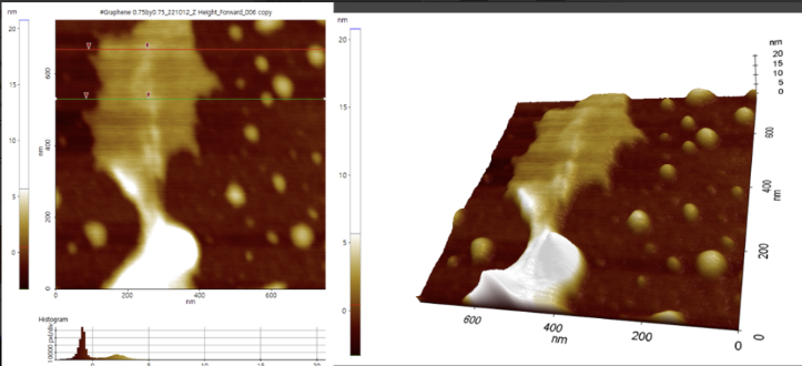
- Characterization of Graphene Composite Materials
To read more on AFM, you can read our Key Tech brochure.
Services
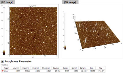
- Surface roughness and morphology analysis
- Imaging scale is 500 nm ~ 100 um.
Pricing
- Regular service: Starts from $300/sample with 3 images. Turnaround time is 4 – 7 days. Expedited service available.
- For a comprehensive overview of our pricing structure, please log in to the Bee Portal.
Equipment
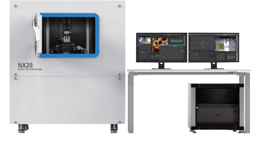
- XY Scanner: 100 μm x 100 μm
- XY Travel Distance: 300 mm x 300 mm
- Z Travel Distance: 25 mm
- Focus Stage Travel Distance: 8 mm
- Vacuum groove holder: 100, 150, 200, 300
mm wafer compatible, small sample
magnetic fixing holder, up to 20 mm thick - Vibration noise levels below 0.5 Å or 0.3 Å RMS

FAQ
A: AFM operates in several modes, including Contact Mode, Tapping Mode (or intermittent contact mode), Non-Contact Mode, and Dynamic Force Mode (or amplitude modulation mode). Each mode offers specific advantages for different applications.
A: AFM is used in materials science for surface topography analysis, measurement of mechanical properties (nanomechanics), investigation of material properties at the nanoscale, and even manipulation of individual atoms and molecules.
A: Yes, AFM is valuable in biology for imaging and studying biological samples at the nanoscale. It can provide information on cell morphology, DNA structures, protein interactions, and more, often in liquid environments.
A: AFM plays a critical role in nanotechnology research by enabling the characterization, manipulation, and fabrication of nanoscale structures and materials. It is essential for understanding and developing nanoscale technologies.
A: AFM measures mechanical properties by applying controlled forces to a sample’s surface and monitoring the deflection of the cantilever. These measurements can include stiffness, adhesion, and indentation properties.
A: Yes, imaging in liquid environments with AFM requires specialized techniques and considerations to maintain sample stability and minimize tip-sample interactions. It is commonly used for studying biological samples and hydrated materials.
A: Variations of AFM include Scanning Tunneling Microscopy (STM) for conducting surfaces, Magnetic Force Microscopy (MFM) for magnetic materials, and Electrostatic Force Microscopy (EFM) for studying electrical properties. Additionally, environmental AFM allows imaging in controlled gas or liquid environments.
A: Force spectroscopy in AFM involves applying a controlled force to the sample and measuring the resulting interactions. It provides information about adhesion forces, biomolecular interactions, and mechanical properties at the nanoscale.
A: Tapping mode AFM is often preferred for delicate samples or when minimizing tip wear is crucial. It reduces lateral forces and is suitable for imaging soft or loosely adherent surfaces.
A: Strategies for optimal AFM imaging conditions include choosing the appropriate mode, optimizing imaging parameters (such as setpoint and scan rate), minimizing external vibrations, and carefully selecting cantilevers and tips for specific samples and applications.

