Customer Service Workflow
01
Consult with our technologists
02
Provide your samples
03
Receive in-depth report
04
Debrief with our technologists
Get a free consultation today!
Contact Us TodayOutermost Technology

6+
Years in Business

50+
Companies Served

150+
Happy Clients

100+
Types of Services

200+
Equipment Available
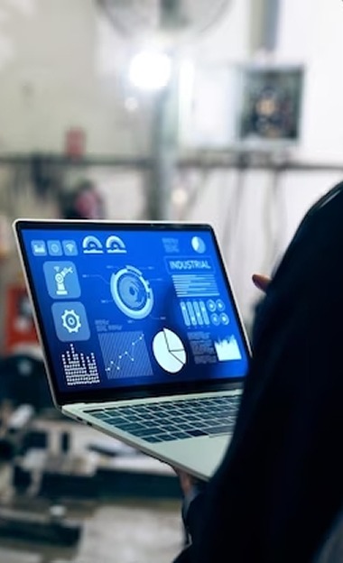
Services

Materials Analysis
• Advanced and Affordable with in-depth analysis
• Good Pricing on high-volume samples
• Solution provider for projects
Reliability Testing
• From environmental to functional tests
• Support for urgent need
• Professional consultation

Reverse Engineering
• Semiconductor devices
• Package, process, and functional block analysis
• Circuit extraction
• Free pre- and post-consultation

Failure Analysis
• State-of-art equipment with highly experienced engineers
• Affordable service pricing
• Free pre- and post-consultation
Key Updates
Materials Analysis
Device Testing
Mar. 2025
Corrosion mechanism analysis of metal strands used for concrete structure
Feb. 2025
Ion chromatography analysis of battery electrolyte
Jan. 2025
Cs-TEM/EDS/EELS analysis of specially coated carbon layer structure on metal substrate
Dec. 2024
Intrinsic voids analysis of Inconel alloy
Nov. 2024
Corrosion on high power bolts/nuts for servers in data center
Oct. 2024
Analysis of green particulates generated in the coolant circulation in data center
Sep. 2024
Thermal property analysis of new graphite material for high temperature use
Aug. 2024.
P and C ratio determination of polymers materials
Jul. 2024
Dynamic SIMS analysis of p- and n- doping profiles in silicon
Jun. 2024
Shelf-life deposition analysis of polymer by GPC
May 2024
High resolution XPS analysis of graphene focused on carbon bonding types
Apr. 2024
Surface morphology analysis of bio-sensors
Mar. 2024
XPS analysis on IC chip to determine corrosivity damage
Feb. 2024
Ferrite material analysis with Cs-TEM
Jan. 2024
CTE measurement of dielectric amorphous films
Dec. 2023
ICP-OES to quantify unknown component elements
Nov. 2023
Polymer characterization with multiple techniques: FTIR, GPC, Raman, TGA, and DSC
Oct. 2023
Ion Chromatography analysis of solvent samples for fluorine in ppb level
Sep. 2023
MALDI-ToF analysis of polymer samples
Aug. 2023
ICP-MS and IC anion analysis for new electrolyte development
Jul. 2023
Unknown particle defect analysis on wafer using TEM-EDS
Jun. 2023
Purity analysis of organic material batch using ICP-MS and IC
May 2023
Cs-TEM-EDS of a bulk copper piece coated with unknown graphene.
Apr. 2023
SEM-EDS on a glass piece to identify defects.
Mar. 2023
X-sectional polishing of LED device for FA at interfaces
Feb. 2023
Nano-scale analysis of onion shape graphene with Cs-TEM
Jan. 2023
EBSD analysis of tungsten film
Dec. 2022
Structure/composition analysis of HEMT by TEM/EDS
Nov. 2022
Two-side Polishing of Micro LED Device
Oct. 2022
Unknown coating material analysis of parts used in plasma process chamber
Sep. 2022
Layer structure analysis of graphene using Cs-TEM
Aug. 2022
Failure analysis of metallized ceramic using 3D CT, CSAM, and SEM-EDX
Jul. 2022
Karl Fisher/FTIR/GC-FID analysis of an organic solvent
Jun. 2022
C-, F-, and H- NMR analysis of organic solutions for graphene
May 2022
XPS analysis for an identification of organic contaminations
Apr. 2022
TEM/EDS analysis on HEMT device
Mar. 2022
Hi-resolution d-XPS analysis for ITO for uLED application
Feb. 2022
C-SAM for advanced wafer bonding technology
Jan. 2022
Device structure analysis using FIB-TEM-EDS analysis of a whole wafer
Dec. 2021
Electrical and structural analysis of high capacitance materials in MIM structure
Nov. 2021
Cross-sectional failure analysis of micro-LED display parts
Oct. 2021
Analysis of biological molecules using Nanoscale FTIR
Sep. 2021
Quantification and identification of fungicidal toxins in fruit
Aug. 2021
Electrochromic device dopant identification and profile using ion milling and SSRM
Jul. 2021
Contaminant analysis of electrolyte solutions using ICP-MS and GC-MS
May 2021
Polymeric structural characterization using Nuclear Magnetic Resonance (NMR)
Apr. 2021
SEM analysis of battery composites
Mar. 2021
Fluorescence measurement of plastic films for research
Feb. 2021
DSC measurement of metal alloys for development
Feb. 2021
Metal composition testing by ICP for alloy development
Jan. 2021
Flash point measurements for solvents for development
Jan. 2021
Ion chromatography of semiconductor samples for failure anlaysis
Dec. 2020
Optical measurements on silver coated mirrors for research
Dec. 2020
LA-ICP-MS for trace metal analysis of semiconductor films for development
Nov. 2020
TGA measurements of polymer samples for development
Nov. 2020
TEM and EDS of LED Device Structures for failure analysis
Oct. 2020
XRR for density and thickness of dielectric films for semicondcutor development
Oct. 2020
XPS Depth profiles of metal oxide films for semiconductor research
Sep. 2020
NMR of polymer samples to measure ligand ratios for polymer development
Sep. 2020
Kelvin probe measurements of LED device structure for research
Aug. 2020
Heated ellipsometry measurements for medical devices for research
Aug. 2020
RBS measurements of ferroelectric thin films for memory development
Jul. 2020
Cross section SEM measurements on coated metals for semiconductor development
Jul. 2020
ToF depth profiles on LED device structures for semiconductor failure analysis
Jun. 2020
Extensive analysis of carbon powerder using TEM/EDS/TGA/XPS/FTIR/SEM for new graphene development
Jun. 2020
TEM+EDS analysis of GaN device structures for power device development
May 2020
Optical profilometry for defect characterization on transparent plastics for nuclear industry
May 2020
Reverse engineering of glue sample using DSC and FTIR for pest control failure anlaysis
Apr. 2020
GC-MS testing for toxicoloy of avocados for food development
Apr. 2020
Nano-FTIR of dielectric films for studying surface bonding for new semiconductor materials
Mar. 2020
M-SIMS depth profiles of doped material for optical telecommunication application
Mar. 2020
EELS Measurements on Dielectric films for semiconductor research
Feb. 2020
TEM/SEM/XRD/Uv-Vis analysis of Ag nanowires for transparent displays application
Feb. 2020
Measuring surface area of carbon powders using nitrogen gas for graphene industry
Jan. 2020
Polymer identification using TGA hyphenated to a GC-MS for semiconductor failure analysis
Jan. 2020
High Resolution ToF-SIMS depth profiles of Magnetic RAM (MRAM) development
Mar. 2025
Hole-decapsulation and high-res imaging of historic IC devices for IEEE Global Museum
Feb. 2025
Reverse engineering of iPhone 16 Pro Max
Jan. 2025
Die-pad search for Logic devices manufactured by a specific fab
Dec. 2024
Decapsulation of IC devices for wire re-bonding
Nov. 2024
Reverse engineering of a PSMC Logic device
Oct. 2024
Reverse engineering of a major CPU product – Logic and IO
Sep. 2024
Reverse engineering of a major CPU product – SRAM and Logic
Aug. 2024
Reverse engineering of a PSMC DRAM device
Jul. 2024
Real time TEM analysis of photonics devices
Jun. 2024
Root cause analysis of a local corrosion on PCBA used in data center
May. 2024
CIS image sensor (SKHynix) design analysis for IP litigation
Apr. 2024
Structure/composition analysis of a BSI CMOS image sensor
Mar. 2024
Row driver analysis of a CIS module from a major manufacturer
Feb. 2024
Gas corrosion testing for PCBAs
Jan. 2024
TSV analysis of DDR4 memory device
Dec. 2023
Failure analysis of slightly opened coil
Nov. 2023
CIS image sensor (Samsung and Sony) design analysis for IP litigation
Sep. 2023
Structure analysis of HBM2 memory device packaging
Aug. 2023
Die imaging of IC device for AI application
Jul. 2023
X-sectional analysis of DDR5 focused on airgap and liner layers
Jun. 2023
Multi-stack CIS image sensors from major brand smartphones
May 2023
TSV structure analysis of DDR5 DRAM device
Mar. 2023
Full process analysis report release of a SoC device of a major brand smartphone
Nov. 2022
Top down high-resolution imaging of fin and gate from 14nm FinFET based device
Sep. 2022
Package and process analysis of SoC used in major brand smartphone
Jul. 2022
3D CT failure analysis of new circuit board stack structure
Jun. 2022
Decapsulation of metal packaged server CPU
May 2022
Contract on the development of a new application of SCM for nano-LED application
Apr. 2022
Die marking imaging for a full SSD products of a major manufacturer
Feb. 2022
Image sensor dopant profile analysis in a smartphone camera of a key manufacturer
Jan. 2022
Charge trap cell structure analysis of NOR and NAND devices from a major manufacturer
Dec. 2021
Identification of top oxide layer on active fin from an advanced DRAM product
Nov. 2021
Extensive reliability testing of a wearable device for health monitoring
Sep. 2021
Comprehensive 5nm FinFET process analysis from Apple A14 AP chip from the 1st biggest foundry and functional block analysis is also done
Aug. 2021
SCM & SSRM scanning, Hall measurement to check Ohmic contact to p-GaN in a nanowire LED device
Jun. 2021
Comprehensive process analysis report for mobile SoC chip having 14nm FinFET process from the 2nd biggest foundry
Apr. 2021
OLED pixel analysis with dopant identification and profiles using Cs-TEM, u-spot d-XPS, and SCM
Mar. 2021
Complete functional block analysis of SSD SoC chips including SRAM size estimation for key
Feb. 2021
Thorough analysis of nanorod structure for u-LED application using Cs-TEM/EDS/EELS
Dec. 2020
High speed SSD (1700MB/s) SoC analysis with its SRAM and metal process
Jun. 2020
Merged contact structure comparison of Sony PS4 Pro, Xbox One X, and Nintendo Switch
Apr. 2020
3D NAND memory structure analysis with planeview and cross-section with Cs-TEM/EDS
Feb. 2020
Layer structure and material analysis of Micron DRAM with 20 nm technology
Sep. 2019
Toshiba image sensor analysis
Dec. 2019
Functional block analysis of Intel SSD SoC for 8TB product
Oct. 2019
Dopant profile and type analysis of Toshiba’s 15 nm technology-based NAND memory by SCM and SSRM
Sep. 2019
Charge trap memory cell analysis of 3D NAND Flash memory
Aug. 2019
65 nm node image sensor analysis used for SONY A9 digital camera
What our clients have to say
The typical solution provider requires that customers be specific about the characterization techniques to be used to analyze their samples. This model of operation is lacking because more than often customers do not know enough about characterization. They can be specifying the wrong techniques and/or missing out on advanced techniques/tools that may provide better answers. Outermost understands as a high level what customers want to know and devises characterization plans to provide answers. They have access to the world’s best and most advanced specialists, techniques, and tools and have provided me with answers, sometimes with methods that I did not know existed or were possible. I recommend Outermost to any engineer or scientist who wants answers.
K. Chan
PhD, Director of Technology, Applied Materials
Outermost has been very helpful, providing us with high-quality, valuable reverse engineering data and analysis in an expedient manner. Highly recommend.
J.W.
PhD, Integration Engineer, IP Licensing Company
I highly recommend Outermost Technology. I have been working with Outermost Technology for the past two years. The team is very professional and they come on-site to present and discuss the results after tasks where completed, which is very appreciated as it is unique in the industry. I highly recommend Outermost Technology.